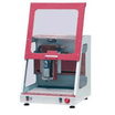
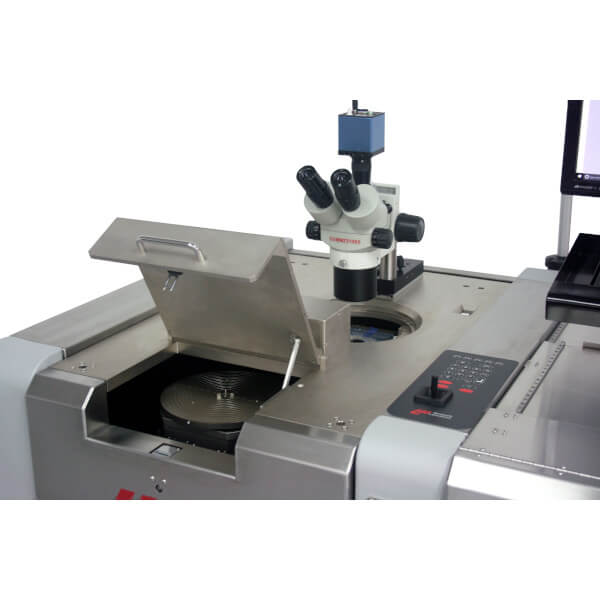
Wentworth A200D Automatic Double-sided Probe Station
Use our chat for technical support or contact us via +45 31 33 18 19 or salg@GOmeasure.dk
- Simultaneous, double-sided probing of wafers up to 200 mm (8″)
- Automatic handling, pattern recognition and probing
- High throughput cassette to cassette automation
- Customizable product enhancing hardware and software options
- Compatible with wide range of industry testers
- Configurable to high voltages in excess of 5 kV for specialized applications
Discover the possibilities
More information
Description
Wentworth A200D Automatic Double-sided Probe Station
PEGASUS™ A200D
AUTOMATIC DOUBLE-SIDED PROBE STATION FOR 200 MM WAFERS
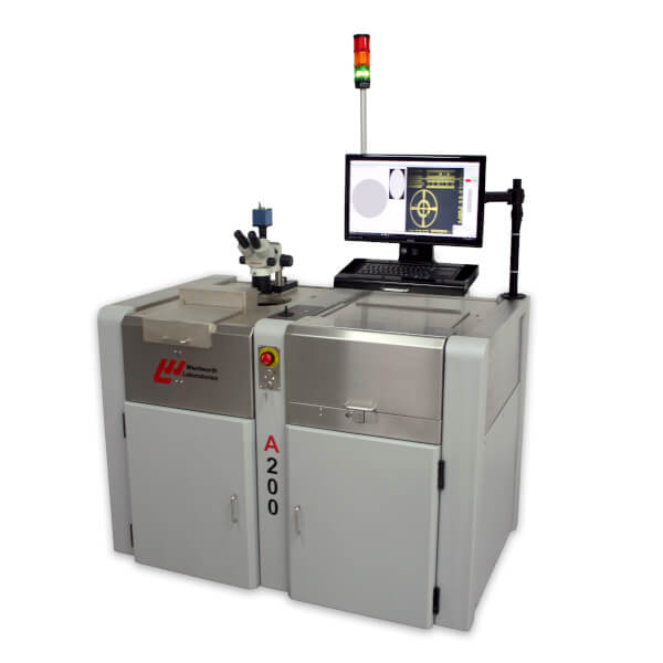
The Pegasus™ A200D series offers simultaneous, double-sided probing of up to 200 mm (8″) wafers in a compact and easy to use fully automatic probing platform. It delivers advanced automation for high volume probing of power devices.
The Pegasus™ A200D features highly developed upper and lower probe arm calipers which can be synchronized to contact the top and bottom side of the wafer at the same time using multiple needle probe cards. A proprietary mechanism ensures a constant pre-set needle load.
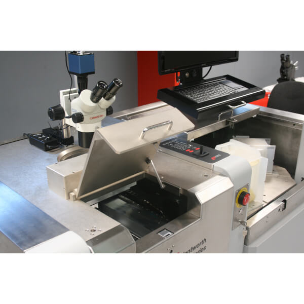
Using proprietary wafer ring clamping chucks, the Pegasus™ A200D has a capacity to load from two cassettes, each containing up to 25 wafers.
WIDE RANGE OF APPLICATIONS
- Double-sided testing of discrete power semiconductors, metal-oxide semiconductor field-effect transistor (MOSFET) and insulated-gate bipolar transistor (IGBT) devices
- Testing of silicon based devices, newer wide-band gap (WBG) materials and compound semiconductors
- Test correlation
VERSATILE AND COST-EFFECTIVE PROBING
To reduce waste and increase yield, this versatile automatic wafer prober can support partial wafers by enabling the user to modify the wafer map in order to prevent testing outside the reduced wafer area.
The Pegasus™ A200D is able to handle thin wafers whilst delivering menu driven, push button control via proprietary LabMaster™ Pro control and monitoring software. LabMaster™ Pro offers an extensive range of control and monitoring parameters. These enable users to operate Pegasus™ A200D series probers at peak performance and include additional advanced features for double-sided probing such as:
- Real-time monitoring and test setup
- Yield analysis of both the wafer and batch under test
- Comprehensive wafer mapping capability
- Image analysis for ink dot and probe mark inspection
APPLICATIONS
Double sided probing is ideally suited for high voltage and high current testing in excess of 5 kV, where backside contact improves test analysis methods. The articulated parallelogram motion of the probe tips ensures that the probes accommodate any deviation in wafer flatness, to ensure even probe marks across the entire wafer. Probe gram force remains consistent to maintain even contact pressure for high levels of accuracy and repeatability.
Kelvin contacts can be used for source and drain to accurately measure resistances and remove lead voltage drop.
Specifications
Documents
Wentworth A200D Automatic Double-sided Probe Station
Wentworth A200D DatasheetOptions
Video
Wentworth A200D Automatic Double-sided Probe Station
PEGASUS™ A200D
AUTOMATIC DOUBLE-SIDED PROBE STATION FOR 200 MM WAFERS
The Pegasus™ A200D series offers simultaneous, double-sided probing of up to 200 mm (8″) wafers in a compact and easy to use fully automatic probing platform. It delivers advanced automation for high volume probing of power devices.
The Pegasus™ A200D features highly developed upper and lower probe arm calipers which can be synchronized to contact the top and bottom side of the wafer at the same time using multiple needle probe cards. A proprietary mechanism ensures a constant pre-set needle load.
Using proprietary wafer ring clamping chucks, the Pegasus™ A200D has a capacity to load from two cassettes, each containing up to 25 wafers.
WIDE RANGE OF APPLICATIONS
- Double-sided testing of discrete power semiconductors, metal-oxide semiconductor field-effect transistor (MOSFET) and insulated-gate bipolar transistor (IGBT) devices
- Testing of silicon based devices, newer wide-band gap (WBG) materials and compound semiconductors
- Test correlation
VERSATILE AND COST-EFFECTIVE PROBING
To reduce waste and increase yield, this versatile automatic wafer prober can support partial wafers by enabling the user to modify the wafer map in order to prevent testing outside the reduced wafer area.
The Pegasus™ A200D is able to handle thin wafers whilst delivering menu driven, push button control via proprietary LabMaster™ Pro control and monitoring software. LabMaster™ Pro offers an extensive range of control and monitoring parameters. These enable users to operate Pegasus™ A200D series probers at peak performance and include additional advanced features for double-sided probing such as:
- Real-time monitoring and test setup
- Yield analysis of both the wafer and batch under test
- Comprehensive wafer mapping capability
- Image analysis for ink dot and probe mark inspection
APPLICATIONS
Double sided probing is ideally suited for high voltage and high current testing in excess of 5 kV, where backside contact improves test analysis methods. The articulated parallelogram motion of the probe tips ensures that the probes accommodate any deviation in wafer flatness, to ensure even probe marks across the entire wafer. Probe gram force remains consistent to maintain even contact pressure for high levels of accuracy and repeatability.
Kelvin contacts can be used for source and drain to accurately measure resistances and remove lead voltage drop.

